|
Home Design Automation Achievements Blocks Features
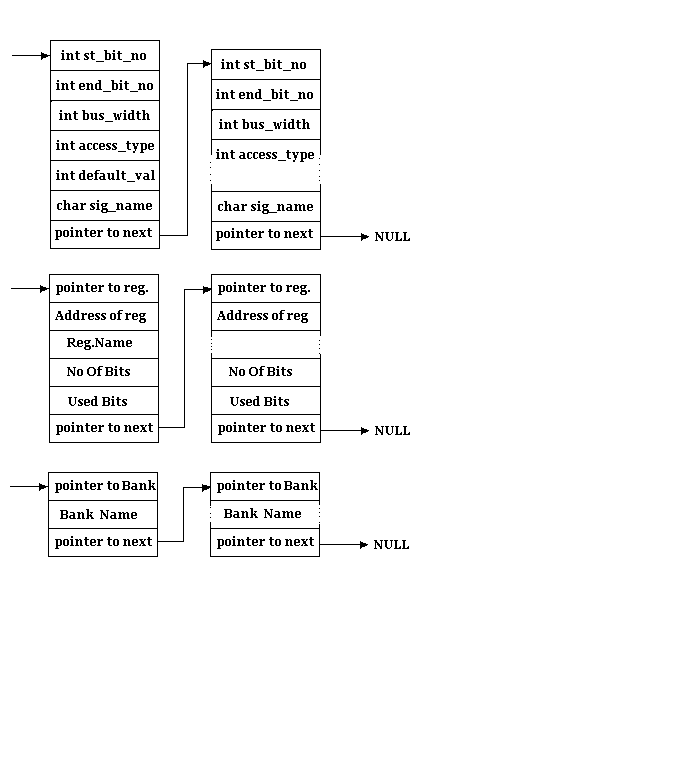
DESIGN OF STORAGE STRUCTURE
As an inseparable part of the design of the
GCI interface the design of the structure required to store the various bank names,
registers within a bank and the leaf level registers of course demands utmost attention.
The basic need of the structure arises because of the need to read the word document in
which the unprocessed data is stored. The design has to meticulously decide upon how to
store the data read from the word document and also the levels of hierarchy during the
formation of the same.
Algorithm for
generation of Linked lists
Verify the number of register banks
Check the number of registers in each bank. Every register is
allocated a unique address and also memory space. We will store all the register banks in
the memory and also all the registers of each individual bank are stored in the memory.
All the register banks will be stored as structures. Each register in a register bank will
be a structure within the structure. A pointer will access individual elements in the
table entries of each register.
Now we can access individual register of a bank
The fields in a single register table are fields in a
structure
Individual Table
- Scan the name of the register
- Move to the appropriate memory address
- In the first row first column of the table get the first
entry. Add one to it to get the number of bits in the table
- See if there is any entry to the right of the first bit. If
‘yes’ then the number of bits for which other description are given in that row
is (No 1- No 2 + 1)
- Check the number of access modes for the register. Check
whether it is RO, RW, RUR, SUR. Make a table of these in the memory.
- Check the access mode for these bits.
- Read the default value of the bit. Here we can limit the
number of entries to either Hex or Binary. If not we can convert all entries ( decimal,
octal, hex ) into decimal.
- The structure will be such that on reading the default value
the signal name associates with those bits be activated & read.
- Function associated with each bit will then be taken into
consideration.
- Process repeated for other rows in a table.
Need of Linked List:
- the basic need of the structure arises because of the need to
read the word document in which unprocessed data is given.
- this information can be stored into a text file on the hard
disc but then the storage area on HD and which is usually smaller than the virtual memory
would limit the maximum register tables.
- the linked lists are stored in the memory. Hence the storage
of this information in memory will be limited by the virtual memory, which is usually
large enough.
- file handling is slower as compared to the memory handling.
Linked lists are in memory.
- Unlike file handling, it is very easy to travel to and fro in
linked list.
Advantages:
- File handling is done once. All required information is read
in one shot. (Efficient file handling),
- Dynamic Memory Allocation is done. (Efficient use of Memory),
- Memory access is faster than file handling (Hence increased
speed)
Validation of log file
The error check is divided into three parts. Bank level error
check, Register level error check and Row level error check. An attempt is made not to
loose the information at any point, if errors are minor. For every error intimation is to
be given to the user so that he can rectify those errors. To store this error list a log
file is generated.
- Bank level Error check:
- If Bank Name is not given then give the temporary Bank Name as
‘NoBankName’. This will be detected if ‘\n’ tag follows word
‘Bank Name’.
Register Entity Name: txpohreg |
Register Bank Type: ** |
Address: 041H |
Bit |
Access |
Function |
DefaultValue |
Signal Name |
Description |
ERROR: Bank Name Not Specified in
table: <Table No.>...Temporary Name Given As: NoNameBank.
- Register Level Error check:
- Register Name:
- If Register Name is not given then give the temporary Register
Name as ‘NoRegName’. This will be detected if ‘\n’ tag follows word
‘Register Entity Name’.
Register Entity Name: ** |
Register Bank Type: TCMD |
Address : 041H |
Bit |
Access |
Function |
DefaultValue |
Signal Name |
Description |
ERROR: Register
Name Not Specified in table: <Table No.>...Temporary Name Given As: NoNameReg000.
- If register name is already existing then an error is given.
That entire table is by passed.
ERROR: An attempt to send a Duplicate Register in table
No. <Table No>
- Address:
- If address is not given, give temporary Address. This will be
detected if ‘\n’ tag follows word ‘Address’. Temporary address is a
Hex value starting with 00H.
Register Entity Name : txpohreg |
Register Bank Type : TCMD |
Address : ** |
Bit |
Access |
Function |
DefaultValue |
Signal Name |
Description |
ERROR: Register Address Is Not Given in table:
<Table No.>...Temporary Address is Given as <Hex number>
- Check duplicate address. For this parse the existing Linked
lists and find out any match with the addresses of existing Registers in all banks.
Firstly go in one Bank, take every Register and its address in that bank. Then go to the
next Bank.
ERROR: Duplicate Register Address is Given in table:
<Table No.>.....Temporary Address is given as<Hex number>.
- Check if all required columns are there or not. After the
Address, columns are expected to follow. Read the entire Row, which is between two
‘\EOR’ tags. Bit, Access Type, Default Value and Signal Name are four required
columns in this Row. Check if they are there or not.
ERROR: Access Column Does not Exist in Table
Number<Table No.>...Hence Skipping the table.
- Row Level Error check:
- Check the sequence of required Columns. This is necessary
because if someone adds more columns in table, then the tool should be able to detect them
and bypass the information written into it. Another advantage of checking the sequence is,
if user gives the columns interchanged then that should not matter.
Register Entity Name : txpohreg |
Register Bank Type : TCMD |
Address : 041H |
Signal Name |
Access |
Function |
Added column |
DefaultValue |
Bit |
Description |
|
|
Unused |
** |
0 |
15-13 |
Unused |
| rdi_code |
RW |
RDI-P Code |
** |
0 |
12-7 |
Code transmitted for
RDI-P |
| Insert_z3_byte |
RW |
Transmit Z3 |
** |
0 |
6 |
When 1, Z3 byte is
transmitted from the user programmable register |
NO ERROR in above table. Bit
and Signal Name columns are interchanged. This sequence is automatically calculated and
the fields are stored accordingly.
- Bit Pattern :
- Check if Bit Pattern is given or not.
Register Entity Name : txpohreg |
Register Bank Type : TCMD |
Address : 041H |
Bit |
Access |
Function |
DefaultValue |
Signal Name |
Description |
| ** |
|
Unused |
0 |
|
Unused |
ERROR: Valid Bit Pattern not found in Register :
<Register Name> of Bank : <Bank Name>...Hence Skipping the Row in table
:<Table No.>
- If given, check if they are some valid numbers or not. Store
the Start bit and End bit numbers in ascending order. Then calculate the width of this
pattern.
- Check for any bit Overwriting from previous bit patterns, if
any,
- Access Types :
- Check if Access Type is Given or not. If the bits are
‘Unused’ then the Access Type is not expected.
- If given, check if they are valid access types. There are four
valid access types; RW,RO,RUR and SUR. The string comparison is done for checking
validation.
- This Access type will be compared with the Access Types of
previous Rows for any mismatch, because the Access Type of all bits in one Register is
same. Hence if any mismatch is found it will be intimated to user and the access type
given in previous row is stored.
- If invalid, take RW as default Access Type.
Register Entity Name : txpohreg |
Register Bank Type : TCMD |
Address : 041H |
Bit |
Access |
Function |
DefaultValue |
Signal Name |
Description |
| 15-13 |
|
Unused |
0 |
|
Unused |
| 12-7 |
** |
RDI-P Code |
0 |
Rdi_code |
Code transmitted for
RDI-P |
| 6 |
** |
Transmit Z3 |
0 |
Insert_z3_byte |
When 1, Z3 byte is
transmitted from the user programmable register |
| 5-0 |
RO |
Transmit F2 |
0 |
Insert_f2_byte |
When 1, F2 byte is
transmitted from the user programmable register |
ERROR: Access Mismatch Found in Register: <Register
No.>
Here the access type of the first used bit-pattern is not
given in table. Hence the default access type is stored as RW. In the last row the access
is RO, which will be a Access type mismatch.
d> Default Value:
- Check if Default Value is given or not,
- If given, check its validity. The default value should be such
that it can be expressed in the given bit pattern length. Example for three-bit wide
pattern 7(binary 111) can be the default value but 8(binary 1000) can’t be.
- If invalid, take 0 as Default Value.
ERROR: Invalid default value is given in table no
<Table No.>. Changing the default value to zero.
- Signal Name :
- Check if Signal Name is given or not,
- If given, check if duplicated. For this parse through the
existing rows of that table and compare the Signal Name. If this signal name exists
before, append _0 to this Signal Name and store it.
ERROR: Duplicate Signal Name Found in Register
:<Register Name>of Bank <Bank Name> in table :< Table No.>...Signal Name
changed to : <Signal Name >_0
- If not given, take ‘NoSig’ as Signal Name.
Block Diagram of the structure
|
|
|