|
|
|
FUNCTIONAL BLOCKS
GENERAL DESCRIPTION:
All the core cells come equipped with user programmable
options and performance monitoring registers. The generic controller interface is designed
to provide a means of accessing these registers through a standard microprocessor
interface. The ?p interface is asynchronous with respect to the microprocessor clock. The
GCI converts the synchronous signals coming from the registers into these asynchronous up
i/p.
The read or write requests on the GCI bus are acknowledged by a ready from the GCI. An
asserting of read indicates that the transaction has been completed. The read or write
requests are to be disserted only after ready has been generated by the GCI. The Generic
Controller Interface or GCI in short comprises of the function blocks shown above. The Rx
GCI and Tx GCI are two blocks opening on the tx clock and the rx clock respectively.
The Top Mux multiplexes the signals between these clock domains.
FUNCTIONAL BLOCK DIAGRAM OF THE GCI:
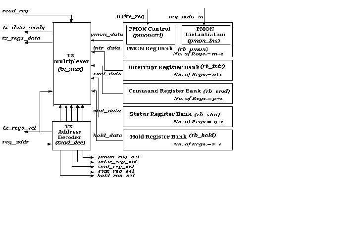
FIG1.0: Scanned image of the generic block diagram of the tool(Transmitter
Part)
Implements the read/write type of registers
Multiplexes the status indications from the core based on address
Implements interrupt register which are reset upon read
8 clocks Read/Write Cycle time
FUNCTIONAL DESCRIPTION
The Generic Controller Interface or GCI in short
comprises of the function blocks shown above. The Receiver (Rx) GCI and the Transmitter
(Tx) GCI are two blocks opening on the Tx clock and the Rx clock respectively. The Top Mux
multiplexes the signals between these clock domains.Functionally the Tx GCI and the Rx GCI
are identical. The Tx GCI is described here. The same description holds true for the Rx
GCI. As shown in figure below the Tx GCI comprises of the Tx Registers and the Tx
Handshake blocks.
TX REGISTERS
The Tx registers block is functionally divided as shown above.
Functions
1. Decode the address to generate internal enables
2. Implement the registers storage elements or register banks
3. Multiplex the data from the register bank based on decoder address
4. Generate a ready for the Handshake block when valid data is available from the register
bank
Tx Address decoder
This block operates when ‘csb’ is asserted. It decodes the address and generates
enables for the Register Banks. The functions performed by this block are listed below
Functions
1. Decode the address to generate register enable
2. Decode the address to generate data bus select signal for the Tx Multiplexer
3. Generate the latch enable for the Tx Multiplier block to latch the data from the
Register Bank
4. Generate valid address detected for the Top level Mux
Register Bank
The register bank comprises of the data storage elements and the Multiplexer.
The Storage Elements
The storage elements are differentiated on the type of register to be
implemented. The types are
1. Performance Monitors 32-bit Counter with rollover
2. Interrupt status register (reset upon read)
3. Read/write configuration register
4. Holding register (latch upon read)
Synthesizable VHDL models are defined for each of the register types for single bit,
4-bit, 8-bit and 16-bit wide. The tool uses the basic registers and only these registers
are used to generate the port-mapped components. These registers are stored in a library
and the tool refers to this library while components are instantiated
Multiplexer
The data from each of the storage elements is multiplexed according to the enables from
the address decoder. Depending on the number of register storage elements the multiplexing
can be done in multiple stages to achieve the desired timing, with each stage being
identical in design.
Tx Handshake
The Tx Handshake block provides a bridge between the transaction requests on the GCI bus
and the Tx Register side bus. It performed the following functions
1. Synchronize the read or write request with the transmitter clock of the CoreCell
2. Generate single clock wide read and write request for the Tx Register block
3. Generate ready for the FCI interface using the ready from the Tx Register block
4. The ready once asserted remains active as long as the read or write requests are
disserted on the GCI bus.
![]()
![]()